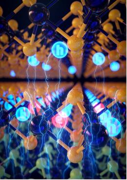
In a paper published earlier this month in Nature Physics, Yongtao Cui, an associate professor of physics and astronomy at UC Riverside, and colleagues report the discovery of a novel electronic state in a new type of moiré superlattice formed by 2D materials.
In conventional semiconductors, electricity is carried by either negatively charged electrons (n-type) or positively charged holes (p-type), the latter being electron vacancies. Cui explained that these two types of charge carriers rarely coexist in the same structure because of their very different energies. The new study succeeded in realizing the coexistence of electrons and holes by designing a moiré superlattice of 2D semiconductors. This new configuration of charge carriers allows scientists like Cui to explore new types of device functionalities not possible in conventional semiconductor materials.
A moiré superlattice is a structure of two or more layers of similar materials stacked together, forming interference patterns that typically arise when one object with a repetitive pattern is placed over another with a similar pattern.
Previously, Cui and colleagues found an electrically insulating state when they got electrons to occupy the moiré superlattice of two monolayers of semiconductors (tungsten disulfide, WS2; and tungsten diselenide, WSe2).
In the new study, the researchers added an extra layer of WSe2 to the moiré superlattice. This added layer does not form a moiré pattern and is, therefore, different from the original WSe2 layer, allowing the researchers to manipulate the distribution of electrons in two WSe2 layers with different properties.
“Interestingly, we found that the electrons with such a distribution can be viewed as one layer hosting electrons while the other hosting electron vacancies or holes, and these electrons and holes could still interact strongly with one another and organize themselves in an ordered manner to form an insulating state that is different from the one we reported in our earlier study in which all electrons are in one layer,” Cui said. “Our new work provides a new platform to engineer electron interactions and explore new device functionalities in 2D materials.”

Cui, who is one of the corresponding authors of the paper and a recent recipient of a CAREER award from the National Science Foundation, was joined in the research by colleagues at Rensselaer Polytechnic Institute in Troy, New York; University of Electronic Science and Technology of China; University of Texas at Dallas; Arizona State University in Tempe; National High Magnetic Field Lab in Tallahassee, Florida; and National Institute for Materials Science in Tsukuba, Japan.
The research at UC Riverside is funded by the National Science Foundation.
The title of the paper is “Excitonic insulator in a heterojunction moiré superlattice.”
In a separate paper published in Nature Communications earlier this week, Cui and his colleagues studied the same device structure but in the case of opposite electron distribution, i.e., all electrons are pushed into one layer of the multiple WSe2 layers.
“This scenario is rather like our earlier study,” Cui said. “We found that the added layers, without any electron occupation, can still influence the interactions among electrons in the adjacent occupied layer, offering a new knob to tune the insulating states previously discovered.”
